David A. Antler
Clever cost-savings on a MUJI interface board
It’s always tempting to see how things are built. I noticed I hadn’t turned on my MUJI diffuser in a few weeks so I decided to have a look on the inside. One fascinating aspect of mass-market consumer products is the desire to make things simple and to reduce cost. This often leads to interesting design choices, as we’ll see.
The device’s industrial design is nice and seamless. In its upright configuration there aren’t any visible screws or fasteners: it’s a plump glowing orb of light and vapor. But turn the unit upside down and three screw holes reveal access to the inside.

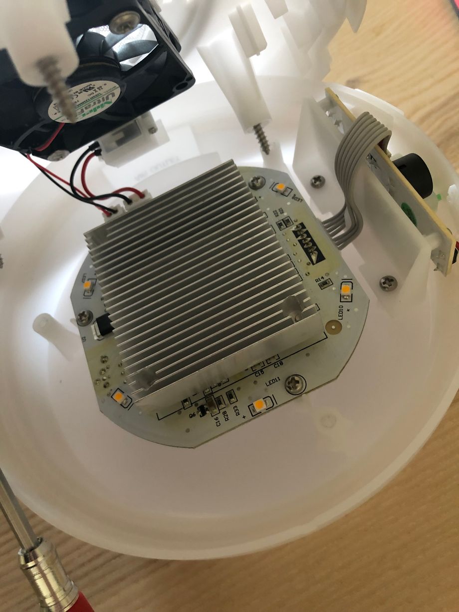
There are four electrical components linked by wires. The 24.5V barrel jack input leads to a pair of wires that hook up to a 3 position JST XH connector on the central board. The central board has a large aluminum heatsink and its connectors fan out into a JST XH 2-pin connector for a fan, and an interesting JST PH connector with 7 pins to an interface board. They’re all tough to remove!
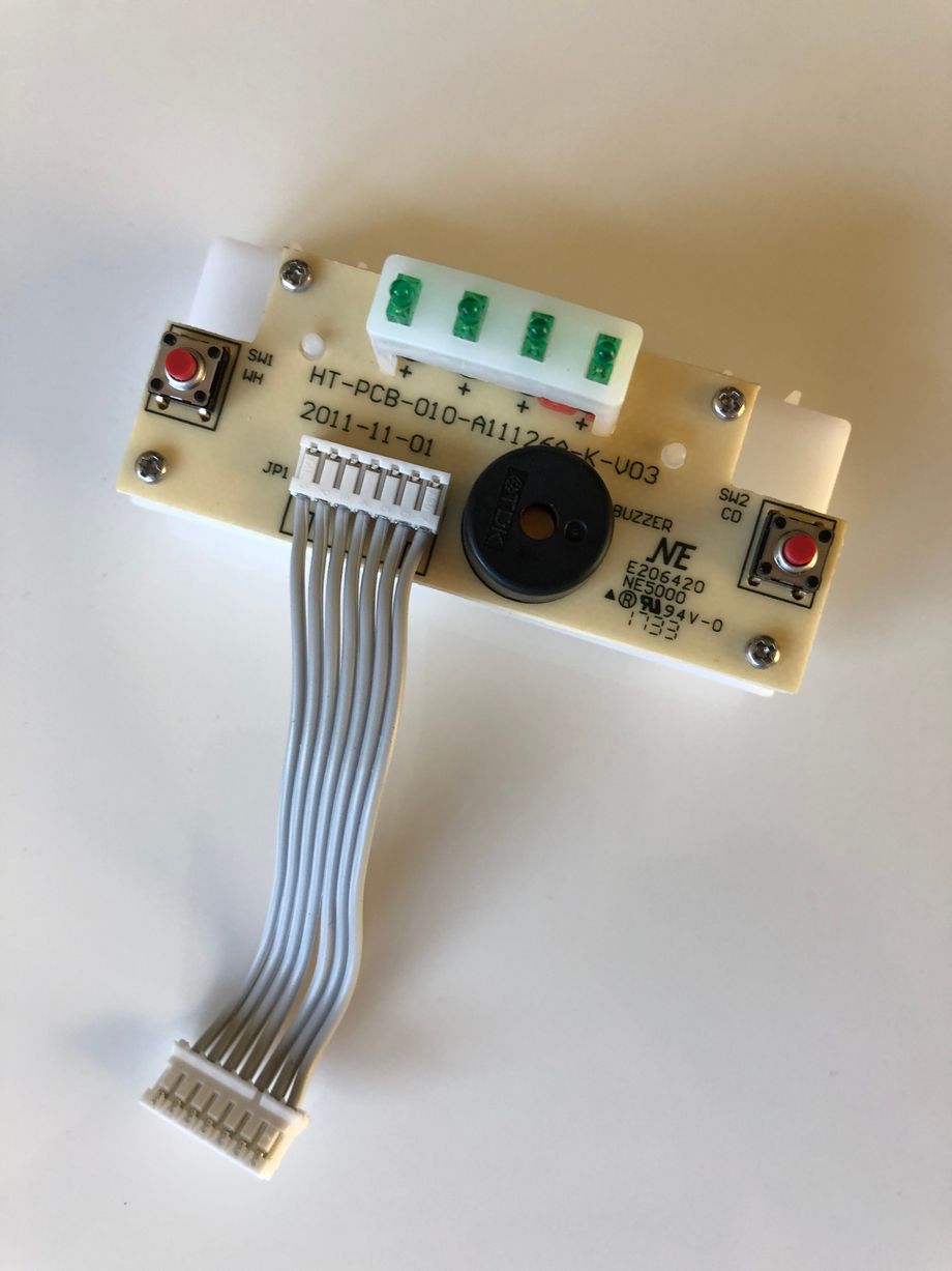
I’m immediately attracted to the interface board. It’s looks quite simple: a single wire bundle going to just four LEDs, two buttons, and a buzzer.

A few cost-saving properties are immediately obvious.
- Each component of this board is part of the human-machine interface. There is no “support” circuitry.
- The board has just one copper layer (on the back).
- All of the components are through-hole and can be soldered quickly by a novice.
- The circuit board is thin and uses a soldered-on wire ribbon instead of a connector. This saves a $0.15 JST PH connector (and its female counterpart) from the BOM (bill of materials).
- The design choice to use only 7 wires for controlling 7 components.
The most intriguing property to me was #5. There must be some trickery going on, since even if all 7 components were wired to a common ground, that would require 8 pins. I decided to probe the board with my trusty multimeter to understand how this is done. Here is the schematic I came up with, scribbled on a bit of MUJI’s excellent stationary.
There are a few discoveries from looking at the schematic:
- JP1 pin 3 appears to be a common ground for the switches and the buzzer.
- The status LEDs have a funny structure where JP1 pins 4 to 6 are used to ensure that just one LED is lit.
Once the circuit is drawn on paper, it’s simple to deconstruct a “truth table” to see how the cleverness in #2 works.
| Pin 4 | Pin 5 | Pin 6 | Meaning |
|---|---|---|---|
| 0 | 0 | 0 | Inactive |
| 1 | 0 | 0 | 30 Minutes |
| 0 | 1 | 1 | 60 Minutes |
| 0 | 0 | 1 | 120 Minutes |
| 1 | 1 | 0 | 180 Minutes |
One other interesting thing about this board is the voltage levels used.
As implied by discovery #1, JP1 pin 3 is apparently a common ground, and I measure a 5V differential across each of the buttons. However, this ground is referenced +19.5V above the rectified ground at the A/C power transformer’s barrel connector.
My spelunking into this device ends here. The +19.5V pseudo-ground is partially a mystery because I’m afraid that attempting to free the central PCB could endanger the watertight seal. If you have a theory for why MUJI built the device this way, please email me!